
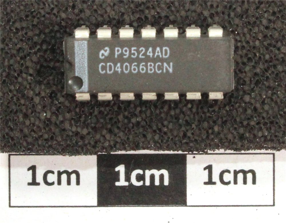
National CD4066BCN Quad Bilateral Switch DIL14
 National CD4066BCN Quad Bilateral Switch DIL14
National CD4066BCN Quad Bilateral Switch DIL14
Manufactured by National Semiconductor - DIP14 through hole package
General Description
The CD4066BC is a quad bilateral switch intended for the transmission or multiplexing of analog or digital signals. It is pin-for-pin compatible with CD4016BC, but has a much lower “ON” resistance, and “ON” resistance is relatively constant over the input-signal range.
Features
Wide supply voltage range 3V to 15V
High noise immunity 0.45 VDD (typ.)
Wide range of digital and ±7.5 VPEAK analog switching
“ON” resistance for 15V operation 80Ω
Matched “ON” resistance ∆RON = 5Ω (typ.) over 15V signal input
“ON” resistance flat over peak-to-peak signal range
High “ON”/“OFF” 65 dB (typ.) output voltage ratio @ fis = 10 kHz, RL = 10 kΩ
Control Line Biasing:
Switch On (Logic 1), VC = VDD
Switch Off (Logic 0), VC = VSS
High degree linearity 0.1% distortion (typ.)
High degree linearity @ fis = 1 kHz, Vis = 5Vp-p,
High degree linearity VDD−VSS = 10V, RL = 10 kΩ
Extremely low “OFF” 0.1 nA (typ.) switch leakage: @ VDD−VSS = 10V, TA = 25°C
Extremely high control input impedance 1012Ω(typ.)
Low crosstalk −50 dB (typ.) between switches @ fis = 0.9 MHz, RL = 1 kΩ
Frequency response, switch “ON” 40 MHz (typ.)
Applications
Analog signal switching/multiplexing
Signal gating
Squelch control
Chopper
Modulator/Demodulator
Commutating switch
Digital signal switching/multiplexing
CMOS logic implementation
Analog-to-digital/digital-to-analog conversion
Digital control of frequency, impedance, phase, and analog-signal-gain