
NXP PCA9511ADP Hot swappable I2C-bus and SMBus bus buffer (Pk of 5)
 NXP PCA9511ADP Hot swappable I2C-bus and SMBus bus buffer (Pk of 5)


NXP PCA9511ADP Hot swappable I2C-bus and SMBus bus buffer (Pk of 5)
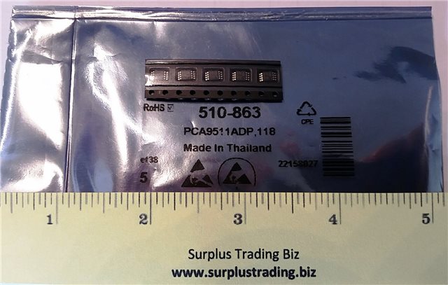
Manufactured by NXP - Part # PCA9511ADP,118
Pack of 5 buffers
NXP PCA9511ADP,118 Hot swappable I2C-bus and SMBus bus buffer in a TSSOP8 Surface Mount package
Supplied in a sealed RS Components package of 5 buffers.
RS Components Part # - 510-863
RoHS Compliant Item
The PCA9511A is a hot swappable I2C-bus and SMBus buffer that allows I/O card insertion into a live backplane without corrupting the data and clock buses. Control circuitry prevents the backplane from being connected to the card until a stop command or bus idle occurs on the backplane without bus contention on the card. When the connection is made, the PCA9511A provides bidirectional buffering, keeping the backplane and card capacitances isolated.
The PCA9511A rise time accelerator circuitry allows the use of weaker DC pull-up currents while still meeting rise time requirements. The PCA9511A incorporates a digital ENABLE input pin, which enables the device when asserted HIGH and forces the device into a low current mode when asserted LOW, and an open-drain READY output pin, which indicates that the backplane and card sides are connected together (HIGH) or not (LOW).
During insertion, the PCA9511A SDA and SCL lines are precharged to 1 V to minimize the current required to charge the parasitic capacitance of the chip.
- Bidirectional buffer for SDA and SCL lines increases fan out and prevents SDA and SCL corruption during live board insertion and removal from multi-point backplane systems
- 2 selectable, fully programmable blink rates (frequency and duty cycle) between 0.172 Hz and 44 Hz (5.82 seconds and 0.023 seconds)
- Compatible with I2C-bus standard mode, I2C-bus fast mode, and SMBus standards
- Built-in DV/Dt rise time accelerators on all SDA and SCL lines (0.6 V threshold)
- Active HIGH ENABLE input
- Active HIGH READY open-drain output
- High-impedance SDA and SCL pins for VCC=0V
- 1V precharge on all SDA and SCL lines
- Supporting clock stretching and multiple master arbitration/synchronization
- Operating power supply voltage range: 2.7V to 5.5V
- ESD protection exceeds 2000 V HBM per JESD22-A114, 200 V MM per JESD22-A115, and 1000 V CDM per JESD22-C101
- 0 Hz to 400 kHz clock frequency
- Operating Temperature -40°C to +85°C